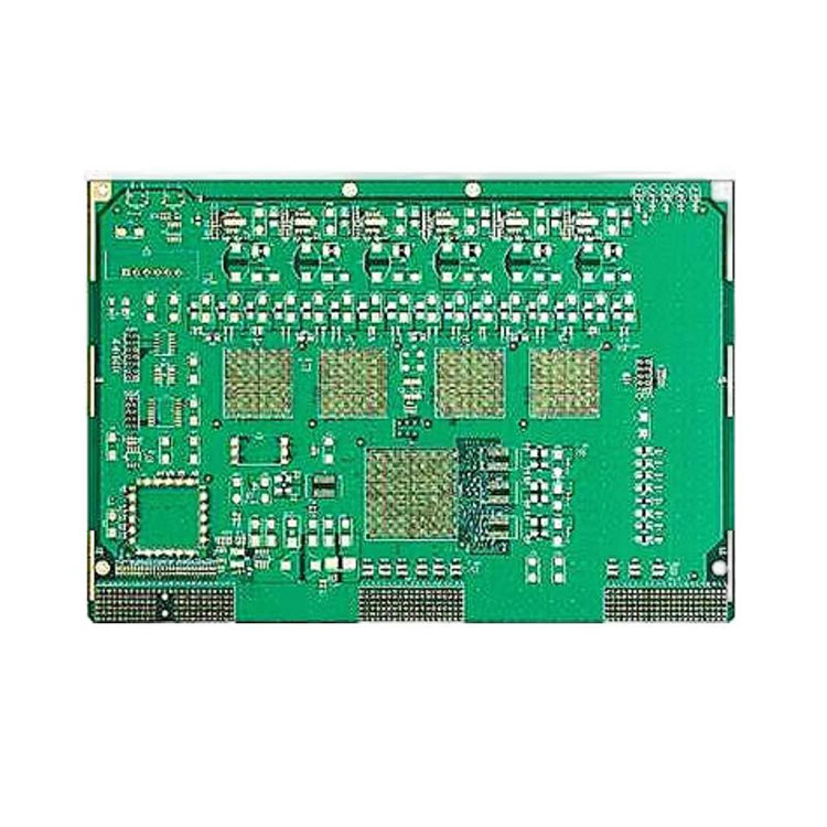
This china 5 Layers PCB Board is a sophisticated electronic part composed of five interconnected layers. Electronic devices rely on PCBs to link electronic components and establish a conductive pathway for electrical signals. Copper, fibreglass, and resin are materials used to create the five layers of a 5 Layers PCB Board. A 5 Layers PCB Board made in china provides numerous benefits such as accommodating more complex circuits, distributing power more efficiently, and minimizing noise as well as signal interference.
A 5 Layers PCB Board is a sophisticated electronic part composed of five interconnected layers. Electronic devices rely on PCBs to link electronic components and establish a conductive pathway for electrical signals. A 5 Layers PCB Board is a rather straightforward correlation between price and board thickness.Thicker boards will cost more than thinner ones, but it also depends on the materials as well. To further elaborate, thicker materials can incur a higher cost to procure, laminate, and form into a PCB.
5 Layers PCB Board’s Basic information:
Surface: HASL/OSP/ENIG/ImmersionGold/Flash Gold/Gold finger ect.
Copper thickness: 0.25 Oz -12 Oz
Material: FR-4,Halogen free,High TG,Cem-3,PTFE,Aluminum BT,Rogers
Board thickness: 0.1 to 6.0mm(4 to 240mil)
Minimum line width/space: 0.076/0.076mm
Minimum line gap: +/-10%
Outer layer copper thickness: 140um(bulk) 210um(pcb prototype)
Inner layer copper thickness: 70um(bulk) 150um(pcb protytype)
Min.finished hole size(Mechanical): 0.15mm
Min.finished hole size (laser hole): 0.1mm
Aspect ratio10:01(bulk) 13:01(pcb prototype)
A 5 Layers PCB Board typically has the following features:
Signal layer 1 (Top layer): Top layer is used for routing the signal traces between components.
Ground plane 1: This layer serves as a ground reference for the signal traces on the top layer.
Signal layer 2: Signal layer 2 is used for routing additional signal traces.
Power plane: This layer provides power to the board components.
Signal layer 3 (Bottom layer): It is used for routing the remaining signal traces between components.