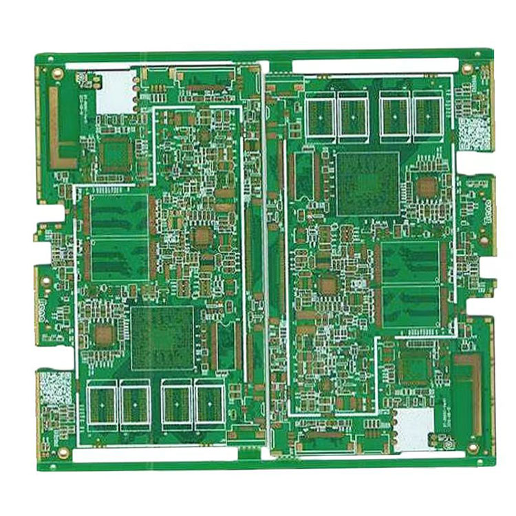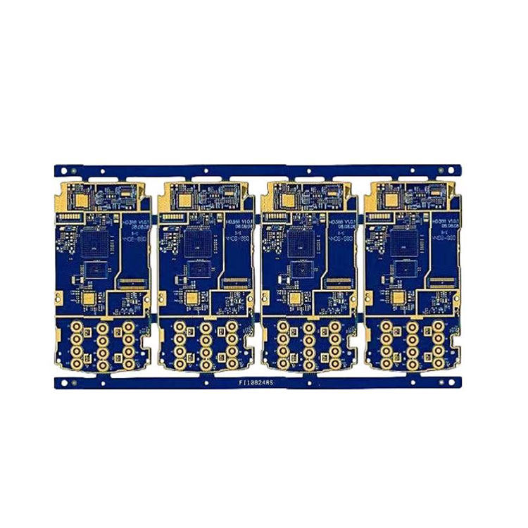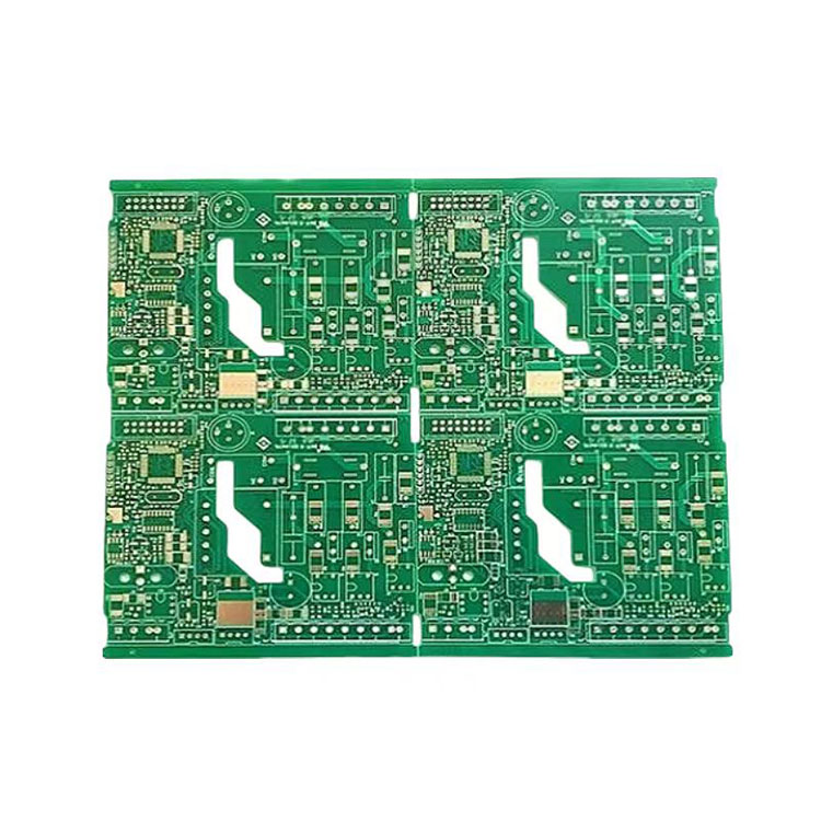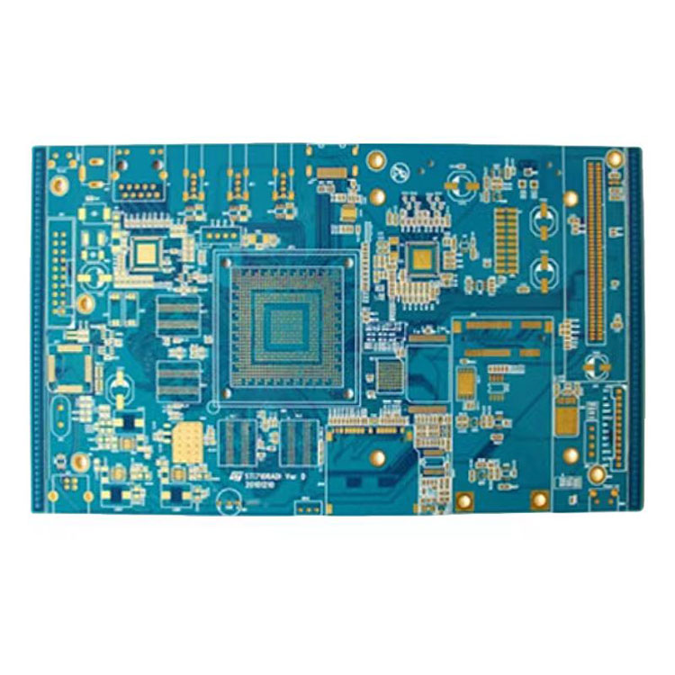
China 8 Layers PCB Board offers us the chance to simply satisfy all of the 5 originally declared objectives. Though many other stack-ups are also possible, we are going to solely discuss a few of them that have proven themselves by providing brilliant EMC performance.Discount 8 Layers PCB Board is sometimes used to improve the EMC performance of the board, not to increase the quantity of routing layers.An 8 Layers PCB Board with 6 routing layers is unquestionably not recommended, no matter how you decide to stack-up the layers.
The 8 Layers PCB Board stack up is a type of Printed Circuit Board (PCB) that has the layers firmly stacked. The stacking goes on to create a formidable dependable and predefined mutual connection among all the layers on the board.It must be noted that the procedure of designing and producing the Customized 8 Layers PCB Board stack up isn’t as easy as mounting the components. Instead, a complex manufacturing procedure is always used to design the 8 Layers PCB Board.
8 Layers PCB Board Description
Layers: 8
Material: FR-4
Solder mask color: Green
Copper thickness: 1oz
Board thickness: 2.0mm
Min. Line width: 0.1mm,
Min. Line spacing: 0.1mm
Surface finish: Immersion gold
Packing: vacuum
Min. drilled hole size: 0.3mm
Certificate: UL, ISO 9001, ISO 14000, TS16949, RoHS
How the 8 Layers PCB Board tends to look like at the end of the design:
Top layer
Prepreg
Ground plane
Core
Inner Layer 1
Prepreg
Power plane
Core
Ground plane
Prepreg
Inner Layer 2
Core
Power plane
Prepreg
Bottom layer


