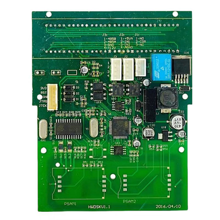
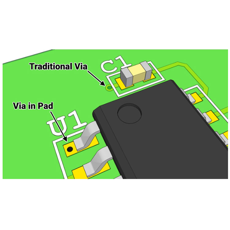
VIA in PAD PCB are essential in multilayer PCB designs as they provide a means for electrical and thermal connections between the different layers of the board. VIA in PAD PCB made in china.Our factory manage VIA in PAD PCB many years. PAD has a welding layer and can be welded by software welding. VIA has no welding layer, and the upper and lower layers are covered with oil. VIA in PAD PCB refers to vias, which can be classified into embedded holes, embedded holes and embedded holes. It is applicable to the connection of transmission lines on different layers of the same Internet, and is generally not used as electric welding components.
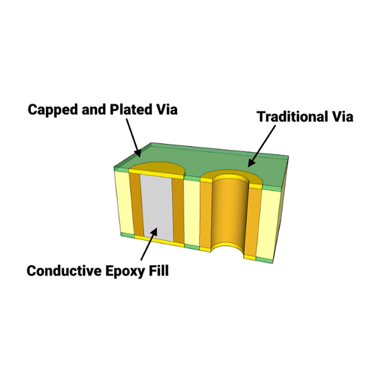
VIA in PAD PCB that pad is called solder layer, which can be divided into pin solder layer and surface mount solder layer; The pin solder layer has solder holes, suitable for welding pin components; We accept Customized VIA in Pad pcb.The surface mount solder layer does not have solder holes, making it suitable for welding surface mount components. The number of holes indicated in the VIA is determined by drilling. Subsequently, it also needs to go through processes such as copper sinking, and the specific diameter will be approximately 0.1mm smaller than the design diameter.
Basic information:
Item name: VIA in PAD PCB
Processing Technology: Electrolytic Foil
Insulation Materials: Organic Resin
Base Material: Aluminum
Surface Treatment: HASL/Immersion Gold/Immersion Silver/Immersion Tin
PCBA Package: Static Packaging, Shockproof Packaging, Anti-Drop
Maximum Board Size: 500mm*1200mm
Transport Package: ESD Bag+Bubble Wrapped +Carton
PCBA Testing Service: PCBA Testing Service
Supplier Type: PCBA Manufacturer
VIA in PAD PCB’s Technical Requirement:
Professional Surface-mounting and Through-hole soldering Technology
Various sizes like 1206,0805,0603 components SMT technology ICT(In Circuit Test),FCT(Functional Circuit Test) technology
PCBA Assembly With CE,FCC,Rohs Approval
Nitrogen gas reflow soldering technology for SMT
High Standard SMT&Solder Assembly Line
High density interconnected board placement technology capacity